
Electro/Photo-luminescence Imaging System
Introduction: By analysing photoluminescence images and data, user can know the impurity doping type and content, energy gap, minority carrier lifetime distribution, identifying material damage, cracks, and defection distribution, etc. PL is the best tool for material composition analysis, performance and quality identification. PL is often used in semiconductor materials, solar cell discrimination, LED epitaxial wafers, and etc.
Specification/Features: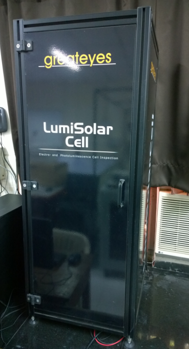
Near Infrared CCD camera -Pixels: > 1000x1000
Quantum efficiency around 70 % or more at 800 nm
measurement on the solar cell of size upto 156 mm x 156 mm
Voltage: 0 to 100 V or higher -Current: 0 to 10 A or higher –
Wattage: 1000 W or higher
Whether facility is open to external users: For the department. Also, used for student lab experiment.
Location:
PV Characterization and Simulation Lab, Short Circuit Lab, Near Hill Side Power House, IIT Bombay, Powai, Mumbai-400076
Contact Details:
In-charge name: Prof. Rajesh Gupta, Dept. of Energy Science & Engineering
Email: rajeshgupta@iitb.ac.in